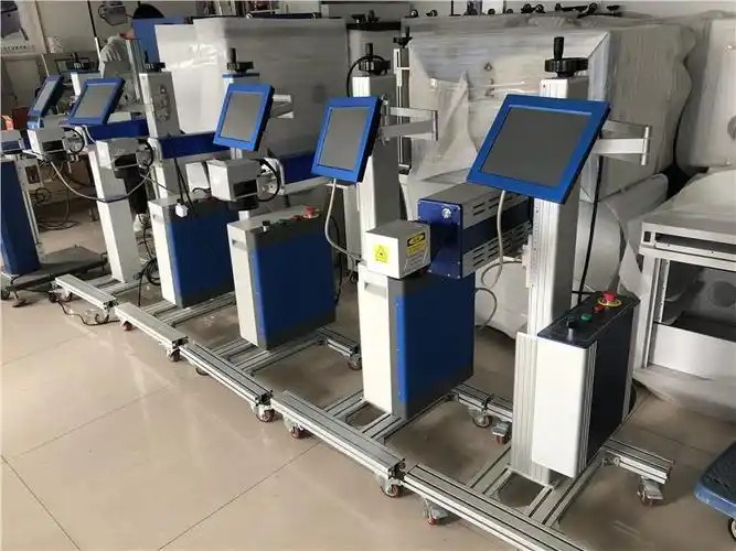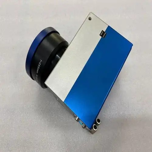
PCB Laser Marking Guide: An Efficient Solution for Product Traceability in the Electronics Manufacturing Industry
As the electronics manufacturing industry continues to evolve toward intelligence, automation, and digitalization, product traceability has become an indispensable part of PCB (Printed Circuit Board) production. From consumer electronics and automotive electronics to medical devices and industrial control systems, more and more manufacturers are adopting PCB laser marking technology to achieve full product lifecycle management and quality traceability.
Compared with traditional inkjet coding and label attachment methods, PCB laser marking offers advantages such as permanent marking, high precision, environmental friendliness, and no consumables. It has become the mainstream identification solution in modern electronics manufacturing.
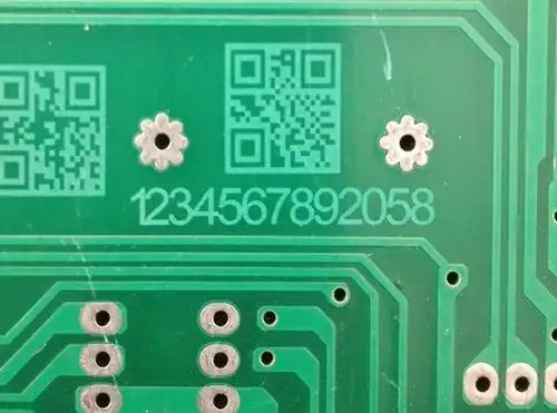
PCB Laser Marking
What Is PCB Laser Marking?
PCB Laser Marking is a non-contact processing technology that uses a laser beam to create permanent markings on the surface of printed circuit boards.
Through a computer-controlled system, the laser can accurately mark:
- QR Codes
- Data Matrix Codes
- Barcodes
- Product Serial Numbers
- Batch Numbers
- Company Logos
- Text Information
- Production Dates
This information can be used for production management, quality traceability, warehouse management, and after-sales service.
Because laser marking does not generate mechanical stress, it does not damage PCB circuits or electronic components.
PCB Material Composition
A PCB (Printed Circuit Board) is a fundamental component used to connect and support electronic components in electronic products. Depending on application requirements, a PCB is typically composed of a substrate, copper foil, solder mask layer, and silkscreen layer.
Among these materials, the most common PCB substrate is FR-4, a composite material made of fiberglass cloth and epoxy resin. It offers excellent mechanical strength, electrical insulation, and heat resistance, making it widely used in consumer electronics, industrial control systems, and communication equipment.
In addition to FR-4, PCBs can also be manufactured using flexible polyimide (PI) materials to produce Flexible Printed Circuits (FPCs), which are commonly used in smartphones, wearable devices, and precision electronic products. For high-frequency communication and RF applications, high-frequency materials such as PTFE (Polytetrafluoroethylene) are often used to ensure signal stability and low transmission loss.
Since PCB surfaces are usually covered with green, black, blue, or white solder masks and contain numerous precision circuits and electronic components, high-precision and low-heat-impact laser marking technology is required for product traceability and identification purposes.
How to Choose a PCB Laser Marking Machine?
Different PCB processing requirements require different laser equipment solutions. Currently, PCB laser applications are mainly divided into two categories: surface information marking and precision PCB processing.
1. PCB Surface Marking – Recommended 5W UV Laser Marking Machine
For most PCB manufacturers, laser equipment is primarily used for permanent marking of QR codes, barcodes, serial numbers, production batch numbers, and company logos.
Since PCB boards are typically made of non-metallic materials such as FR4 and FPC, feature dense circuitry, and require minimal heat-affected zones, UV laser marking machines have become the industry’s most popular choice.
With a wavelength of 355nm, UV lasers provide a cold processing effect, enabling high-precision marking without damaging PCB circuits or electronic components.
They are particularly suitable for:
- PCB QR code marking
- Data Matrix code marking
- Serial number traceability systems
- Online SMT production line marking
- FPC flexible circuit board marking
- HDI high-density circuit board marking
For most PCB surface marking applications, a 5W UV laser marking machine can fully meet production requirements while balancing marking quality and equipment investment costs. It is currently the most widely used solution in the electronics manufacturing industry.
2. PCB Circuit Engraving and Micro-Hole Processing – Recommended 50W or Higher Fiber Laser Marking Machine
With the advancement of laser processing technology, more and more companies are applying laser equipment to PCB circuit processing rather than limiting its use to surface marking.
In R&D, small-batch production, and specialized processing applications, fiber laser equipment can be used for:
- PCB circuit engraving
- Copper layer removal
- PCB micro-hole drilling
- Fine graphic processing
- Conductive layer trimming
- Rapid PCB prototyping
These applications require higher laser power and energy density, so a 50W or higher fiber laser marking machine is generally recommended.
Compared with traditional mechanical drilling and chemical etching processes, laser processing offers advantages such as higher precision, faster speed, no tool wear, and greater automation. It is especially suitable for high-precision electronic products and rapid prototyping requirements.
For companies that need circuit engraving, micro-hole processing, and metal component marking, a 50W fiber laser marking machine can provide higher efficiency and broader application capabilities.
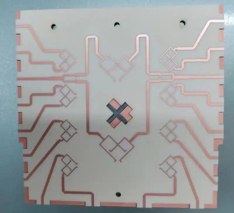
PCB Laser Engraving Sample
Typical Applications of PCB Laser Marking
Consumer Electronics
Used for:
- Smartphone motherboards
- Tablet PC motherboards
- Smart wearable devices
- Communication equipment
Automotive Electronics
Used for:
- ECU control modules
- BMS battery management systems
- Vehicle sensors
- ADAS systems
Medical Electronic Devices
Used for:
- Medical testing equipment
- Medical control modules
- Medical sensors
Meeting strict product traceability requirements.
Industrial Control Systems
Used for:
- PLC control boards
- Industrial circuit modules
- Automation control equipment
Improving equipment management efficiency.
PCB Laser Marking Process
Taking a desktop UV laser marking machine as an example, the PCB laser marking process is usually very simple and can be used for mass production after basic operator training.
Step 1: Import Marking Content
Import the information to be marked into the laser marking software. The system can also be connected to MES, ERP, and other production management systems to achieve automatic data generation and code assignment.
Step 2: Place the PCB Board
Place the PCB board on the working platform and secure it using a positioning fixture.
For mass production applications, automatic conveyor systems, vision positioning systems, and automatic loading/unloading equipment can also be integrated to achieve fully automated marking.
Step 3: Adjust the Focal Length
Adjust the laser head up and down using the adjustment knob until the desired marking result is achieved.
A correct focal position ensures clear QR code edges, complete characters, and a reduced heat-affected zone, resulting in higher marking quality.
Step 4: Set Marking Parameters
Configure laser parameters according to the PCB material and marking requirements, including:
- Laser Power
- Marking Speed
- Frequency
- Fill Spacing
- Number of Passes
For QR code marking on FR4 circuit boards, low power and high-speed settings are typically used to avoid affecting circuits and components.
Step 5: Start Laser Marking
After confirming the parameters, start the machine. The laser beam follows the preset path to complete the marking process.
The entire process is contact-free, produces no mechanical stress, and does not damage the circuit structure.
Under normal circumstances, a single QR code can be permanently marked within just 1–3 seconds.
Step 6: Quality Inspection
After marking, barcode scanners or vision inspection systems are used to verify QR code readability and marking quality.
Inspection items mainly include:
- QR Code Recognition Rate
- Character Clarity
- Marking Position Accuracy
- Contrast Grade
- Data Accuracy
After passing inspection, the PCB can proceed to SMT assembly, functional testing, or subsequent assembly processes.

UV Laser Marking Machine
Conclusion
As the electronics manufacturing industry continues to increase its requirements for product traceability, automated production, and quality management, PCB laser marking technology has become an essential part of modern PCB manufacturing.
Compared with traditional inkjet coding and labeling solutions, PCB laser marking offers significant advantages including permanence, high precision, low maintenance costs, and environmental friendliness.
Whether in consumer electronics, automotive electronics, medical electronics, or industrial control equipment manufacturing, laser marking enables more efficient production management and product traceability.
For electronics manufacturers pursuing high quality and smart manufacturing, PCB laser marking is undoubtedly an important choice for the future.
Contact Us
ZS Machinery specializes in laser marking, laser engraving, and industrial laser solutions, providing professional laser marking equipment for PCB manufacturing, electronics assembly, and smart manufacturing industries.
If you are looking for a laser marking solution for PCB QR code marking, serial number marking, or automated production line integration, feel free to contact us for professional advice and a customized quotation.
Laser Marking Gold Guide